The silicon chip, or integrated circuit (IC), is one of humankind’s most magnificent, complex, and transformative creations.
The IC itself is a silicon sandwich made up of many transistors (little switches) wired together into electrical circuits. Since Robert Noyce and Jack Kilby’s coinvention of the IC in 1958-59, relentless improvements in transistor density have taken place. You could see this change in spacecraft, aviation, communications, and, most obviously for most of us, in the consumer products of their times. In the early days of ICs, for example, one of the earliest products was the basic four-function 1973 Sears/Bowmar handheld calculator. Sixty years later, the hot consumer product is a voice activated smartphone connected to the “world brain” of the internet—science fiction only a generation ago.
From our partners:
BIGGER AND BETTER
It took a long time to get there, but the progress was steady: since Fairchild Semiconductor chemical engineer Gordon Moore first wrote about ICs in 1965, roughly every 18–24 months the number of transistors on an integrated circuit has doubled. The basic process that has allowed this is photolithography, which, if you break it down into its Greek origins means “writing on stone with light.” Figure 1 below shows the general idea.
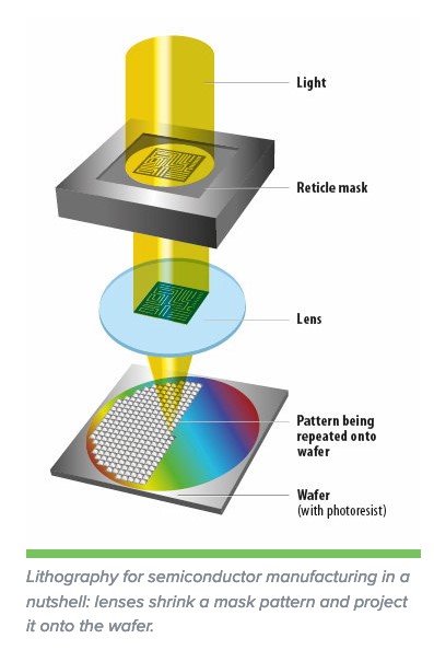
Light (often ultraviolet) is blasted through a stencil with the patterns IC designers want burned into the chip. Special chemicals are applied before and after to allow this and the process is repeated until a sandwich, made up of many layers, has been built up and the IC is finished and ready for packaging.
THE WORLD’S BIGGEST CHIP
Computer designer Gordon Bell once noted that getting the highest speed possible in computers—which rely entirely on ICs—is often about “plumbing and packaging.” Since integrated circuits get hotter the faster they run, fast computers have to worry about keeping their chips cool. We can see this limitation echoed this in the observation that several of legendary supercomputer designer Seymour Cray’s patents were related to ways of keeping his world-beating computer systems cool. For Cray, who always pushed the limits of the possible, keeping the system from burning up was just as important as designing fast circuits.
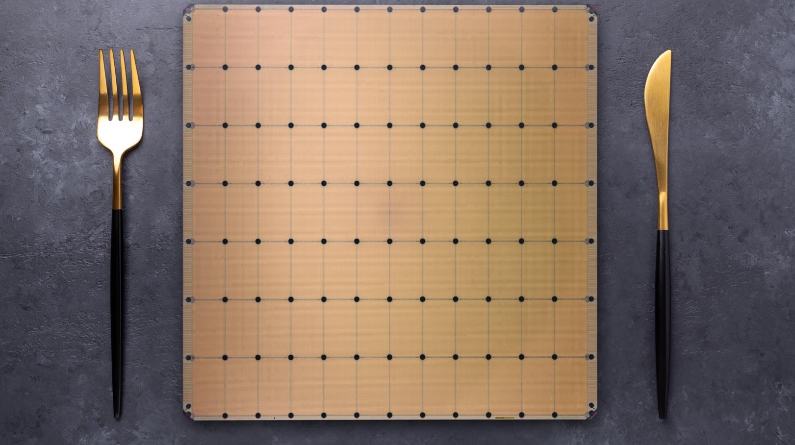
Cerebras, a well-funded Silicon Valley startup, has developed one of the most ingenious and technically elegant solutions to the problem of both “cramming” (to paraphrase Gordon Moore) more transistors onto a chip while keeping it cool. How far could things be pushed? The answer is astounding: on a huge, single square piece of silicon, about 8.5” on a side, the Cerebras Wafer-Scale Engine (WSE) has 2.6 trillion transistors, which make up 850,000 AI-optimized processing units. (Figure 2.) The size of a transistor in the WSE is 7 nanometers. Human DNA is 2.5 nanometers. There are more transistors—by far—in this one Cerebras chip than in all 100,000 computing objects combined in the Museum’s permanent collection.
What’s clever about the WSE is that its design and manufacturing largely follow existing industry processes and methods. Their unique genius was in providing a state-of-the-art ecosystem for the WSE to live in—one which supplied it with power, cooling, and communications.
PROCESS IMPROVEMENT
To pull this off Cerebras relies not on some exotic new method or technology but on existing semiconductor fabrication processes—just modifying them slightly. (The 8.5” on a side footprint, for example, is what’s left when you take a standard 300 mm wafer and cut it into a square).
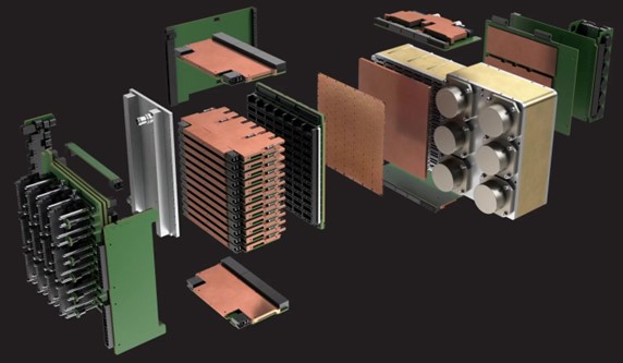
Taking these threads—packaging, cooling, and transistor density—what does this amazing chip look like when packaged up? (Figure 3) The WSE itself is in the center, looking rather delicate among some pretty hard-core hardware. This surrounding technology though is key to the WSE functioning since it both connects the WSE to the outside world through some very serious connector systems, pumps water through cold plates that it touches to keep it cool (Bell and Cray again), and provides a stunning 20 kW of electrical power to supply those trillions of transistors. That, by the way, is enough power to supply about five US homes. That sounds like a lot, but it’s actually only a few billionths of a watt per transistor. These are the kind of engineering problems you have to solve when you shrink racks of ordinary computers down to a single chip.
The scale, ambition and performance of the Cerebras Wafer-Scale Engine is almost beyond imagining.
SPEED, SPEED, SPEED
With all this attention to massive integration (putting everything on one giant chip and packaging it efficiently) a typical Cerebras system is about 1/10th the size of an equivalent computer system using the “ancient ways” of wiring up hundreds of thousands of chips together on separate circuit boards, in separate cabinets, and then wiring those together. When asked why he did not favor using multiple small processors in his supercomputers, legendary computer designer Seymour Cray quipped, “What would you rather have pulling your plow? One large bull or 64 chickens?”
So what are these trillions of transistors in the WSE used for, you’re wondering?
The killer app of the WSE for AI is in reducing neural network training time—the networks that make AI “intelligent.” The WSE can take something that takes other computers weeks and get results in minutes.
The result of this gigantic reduction in training time means answers to AI-powered experiments can come in minutes or hours, not days. This speeds up drug discovery, can model potential cures for cancer, do image processing and work in dozens of new AI-inspired applications that our world will need to face the challenges of the future.
Since so much of the world to come will be shaped by AI-based technologies as time goes by, the WSE is a great milestone to collect, which is why the Museum is particularly happy to bring an example of this amazing device into its permanent collection. The WSE will be on display for a limited time just off CHM’s main lobby starting August 3, 2022. Please visit and see this rare device in person. You will be amazed.
This feature was originally appeared in Computer History.
For enquiries, product placements, sponsorships, and collaborations, connect with us at [email protected]. We'd love to hear from you!
Our humans need coffee too! Your support is highly appreciated, thank you!