As traditional Moore’s law improvements slow down, we are now turning to custom chips to continue improving performance and efficiency. Innovations like Google’s Tensor Processing Units (TPUs) and Video Coding Units (VCUs) have been incredibly valuable at sustainably meeting the growing demand for machine learning and video distribution services, and we expect to see additional custom chips that meet the emerging needs of our customers and users.
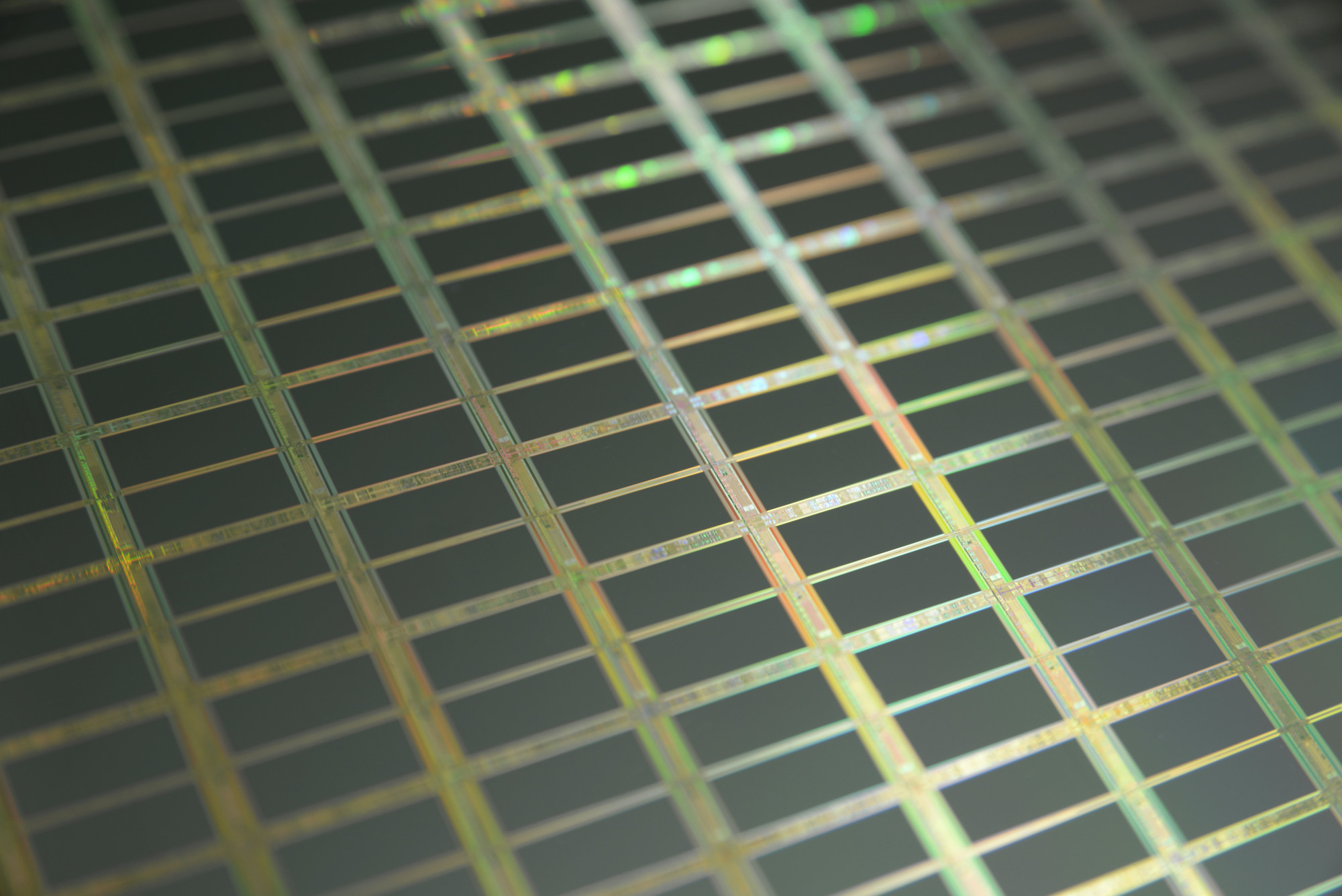
But building custom chips is a complex and costly endeavor. In particular, the semiconductor industry faces a key challenge. Each successive generation (technology node) is achieving more modest benefits, often surpassed by the high costs of manufacturing the chips (e.g., semiconductor mask costs). As one example, after decades of improvements, the cost-per-bit of SRAM memory on our TPUs started increasing with new technology nodes starting with recent generations. To address these challenges, the industry is shifting away from giant monolithic chips. Instead, chip designers are adopting alternate approaches that combine several small chiplets into a single package.
From our partners:
Chiplets come with several advantages. Their reduced die size improves yields and costs, but when connected and packaged together, chiplets can still provide the illusion of a large monolithic chip. The opportunity to mix-and-match different “building block” chiplets allows customized solutions to be quickly developed for different usage models. Additionally, different IP blocks can be manufactured in different process technologies best suited for the function: for example, input/output (I/O) blocks can be manufactured in older process technologies while performance-sensitive compute blocks can be built on the latest technology generation. Such heterogeneous technology matching can avoid the long delays associated with migrating the full IP portfolio to the leading technology node.
However, chiplets also come with several challenges: increased complexity and costs for packaging and testing; potential power, area, and performance overheads associated with disaggregating the design over multiple chiplets; and increased supply chain complexity. Additionally, higher levels of the systems stack (e.g., operating system and scheduling subsystems) may need to become “chiplet-aware” to optimize for the added heterogeneity.
To realize the promise of chiplets and address their challenges, we believe that we need a broader chiplet ecosystem that adheres to a few key principles that we have historically seen to be effective:
- The ecosystem needs to be open. Chiplet IPs need to be interoperable across different vendors and foundries, and support multiple process nodes (both mature and leading-edge) and packaging technologies. The ecosystem needs to support diverse customer use-cases, with reduced friction to customization, and support broad industry engagement and contribution.
- The ecosystem needs to support complete end-to-end specifications including standardization across interfaces, protocols, packaging, testing, and manufacturing, to meet aggressive customer use-cases. For example, for some accelerator use-cases, the physical layer (the chiplet die-to-die interface) needs to support Tbps/mm bandwidth densities at nanosecond latencies and sub-pJ/bit energy efficiencies. Similarly, advanced cost-effective packaging options need to be supported including 3D integration. Likewise, the protocol stack needs to support PCIe, CXL, Arm® AMBA®, and other extensible custom solutions.
- The ecosystem needs to address system-level aspects such as physical form factors, but also security, manageability, and reliability. Common interfaces are needed for discovery, configuration, monitoring, and out-of-band management. Chiplets need to be established with 100% trust on every boot, with appropriate cryptographic key exchanges with roots-of-trust. In-situ (in-system) testing and repairability is important from a quality and reliability perspective. Standardized physical footprints (standardized die-areas, common naming convention, choice of interposers, compatible power supplies) are important to drive common mechanical dimensions for easy system and package integration.
Google has a long history with open and standards-based ecosystems, and we are committed to fostering similar open ecosystems for chiplets as well. We have been investing in open standards through our leadership in the Open High Bandwidth Interface (Open HBI) die-to-die interface standard and publishing the OpenChiplet specification to define a layered architecture for interoperable chiplets. Today, we are pleased to come together with other industry leaders to collaborate on Universal Chiplet Interconnect Express (UCIe) in service of a multi-vendor interoperable chiplet marketplace for the industry.
We are at a critical inflection point in the semiconductor industry, one of the most significant changes since the launch of microprocessors as a building block in the 1970s. Navigating this transition will require leaders across the stack from semiconductor manufacturing, assembly, and test vendors, IP development, silicon engineering, and cloud/infrastructure providers to come together on an end-to-end standard and build a vibrant thriving chiplet ecosystem. We invite the community to join us on this journey as we work together to build the foundation for a new era of specialized and sustainable computing to solve the world’s most challenging problems.
Thanks to Andy He, Rohit Mittal, Mudasir Ahmad, Igor Arsovski, Amber Huffman, Ben Kerr, David Patterson, Ravi Rajwar, Nick Stevens-Yu, Amin Vahdat, Maruthy Vedam for their input to this blog.
Arm and AMBA are registered trademarks of Arm Limited (or its subsidiaries) in the US and/or elsewhere.
By: Parthasarathy Ranganathan (VP Technical Fellow, Google)
Source: Google Cloud Blog
For enquiries, product placements, sponsorships, and collaborations, connect with us at [email protected]. We'd love to hear from you!
Our humans need coffee too! Your support is highly appreciated, thank you!